


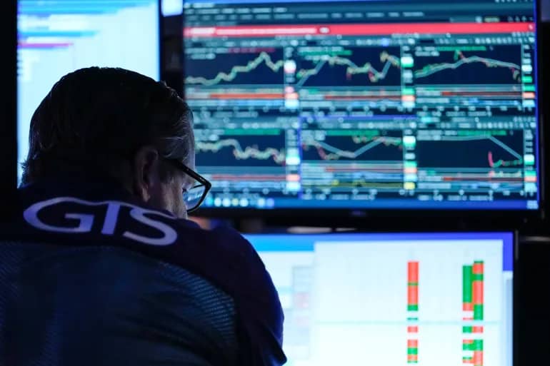
US stock market hits record high amid hopes for Strait of Hormuz reopening
Oil prices fall as US officials tout progress in talks to reopen critical waterway.
5 Aug 2026, 7:38 AM - Digest
Trending
Digest - 5 August 2026 - 10:04 AM
Samsung
The world's largest memory chip manufacturer chose this year's Future of Memory and Storage (FMS) conference in Santa Clara, California, to introduce its V10 Bonding V-NAND, or BV-NAND, prototype. The chip features more than 400 layers and a new wafer-bonding architecture to increase storage density and boost performance.
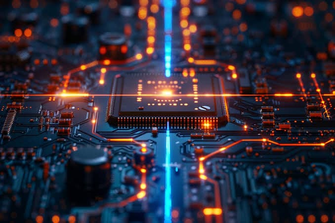
As AI workloads have expanded beyond training large language models to the process of generating answers to user queries, demand for high-capacity NAND memory has increased. NAND flash memory is used to store data such as photos, videos and applications in devices including smartphones.
The company said its BV-NAND technology increases memory density by about 58% from its previous V9 NAND while improving read, write and input/output performance to meet growing demand from AI systems requiring higher-capacity and more power-efficient storage.
Samsung also showed concept models of what it described as the industry's first zHBM and zNAND-O architecture, outlining its vision for next-generation 3D memory that stacks memory cells vertically to pack in more data.
Oil prices fall as US officials tout progress in talks to reopen critical waterway.
5 Aug 2026, 7:38 AM - Digest
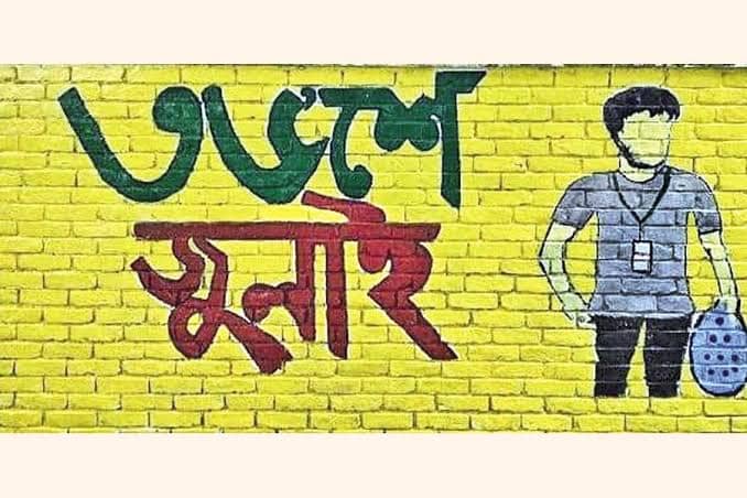
On August 5, 2024, former Bangladesh Prime Minister Sheikh Hasina resigned and fled to India via a military helicopter
5 Aug 2026, 6:51 AM - Digest

This is a comprehensive test article designed to test the CMS and frontend components of Beyond Headlines.
5 Aug 2026, 6:26 AM - Digest

The foundations of modern design systems were laid long before the digital era. From Gutenberg's printing press and reusable woodcut blocks to today's Figma components and design tokens, the core principles of consistency, readability, and scalability have remained remarkably unchanged.
4 Aug 2026, 7:37 AM - Digest


